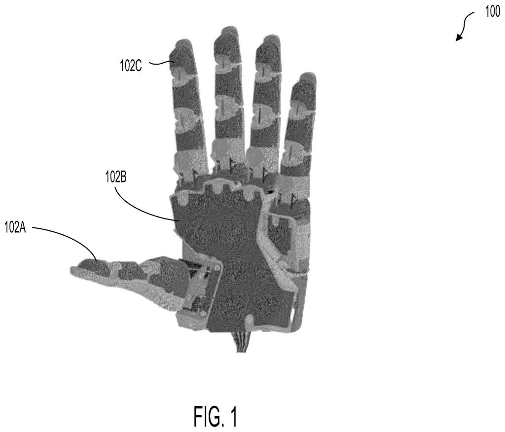
A patent application published on 8 October describes a three-layer tactile array built on TPU, PET or polyimide, shaped into fingertips and palms by thermoforming — with two build orders and five ways to lay the conductors.
A camera tells a robot where an object is. It says nothing about how hard the hand is pressing, or which part of the finger is taking the load. That gap is usually described as a sensing problem. The application Tesla published on 8 October 2026 treats it as a manufacturing problem instead: how do you put a sensor array on a compound curve, at volume, without gluing a flat sheet onto a shape it does not fit.
What the filing describes
Three layers. Two flexible substrates carry patterned conductive regions; a compressible separator sits between them; wherever a top and a bottom region overlap, the stack forms a sensing pixel. The separator material decides the modality — a dielectric separator gives a capacitive pixel whose gap closes under load, a piezoresistive one gives a resistive pixel. Substrates are named as thermoplastic polyurethane, PET or polyimide, and a flexible circuit board carries the signals out. The finished skin can sit on a hard or soft backing under a protective layer.
Two build orders
The claims cover both sequences, which is the part worth reading:
- Stack first, then shape. Print or etch the conductors on flat sheets — screen-printed conductive ink, or laser-cut channels filled with conductive paste — bond them with the separator between, then thermoform the whole stack: heat above the glass transition temperature, press into a mould, cool.
- Shape first, then wire. Mould the substrate into the target form, then lay conductors on the curve. The filing lists nozzle dispensing driven by a CNC stage, laser direct structuring with subsequent plating, and pad printing with a deformable silicone pad.
Either way the array ends up as part of the geometry rather than something bent over it. The abstract states the intent plainly: the sensors can conform to curved geometries and measure surface force, touch and pressure.
“3D” here means shape, not three axes
In robotics literature a “3D tactile sensor” usually means a pixel that resolves normal and both shear components. That is not what this is. The third dimension in this filing is the physical curvature of the part; the sensing is of contact and pressure. Analysts who have read the full document make the same point, and it matters when comparing it against arrays that genuinely decompose shear from a pressure pattern.
What the document does not contain
No sensitivity, no pixel pitch, no hysteresis, no cycle life, no per-part cost. The filing has 20 claims, claims priority from a provisional filed on 4 April 2025, and was filed on 11 September 2025. A published application is a description of a method its authors believe is manufacturable; it is not evidence that a part meeting a specification exists. It also does not name a product — the geometry is consistent with a humanoid hand, but consistency is not a statement of intent.
Why the thermoforming step is the interesting claim
Forming a laminated film over a compound curve strains every layer at once. The conductors stretch or wrinkle, the separator thins where the curvature is tightest, and the pixel area that was 2 mm square on the flat sheet is no longer 2 mm square on the part. Two sensors cut from the same sheet and formed over different moulds will not read the same unless each is calibrated after forming. That is the failure mode anyone hits when forcing a flat array onto a curved surface, and it is why calibrating on a platen and then installing is a procedure that produces confident, wrong numbers.
The filing’s answer is to make the sensor’s geometry the part’s geometry. Whether it holds up is an empirical question the document does not answer: how much the separator recovers after being pressed in the mould, how repeatable pixel position is part-to-part, and whether a capacitive pixel at fingertip scale retains a usable baseline once its electrode area shrinks — that last one has been the central obstacle in published high-density tactile work, where stacking extra electrodes inside the same footprint is used specifically to recover baseline capacitance.
For anyone specifying pressure mapping rather than robot skin, the transferable idea is narrower and still useful: when the measurement surface is curved, the array should be made for that surface, and calibration belongs after forming. A flat-calibrated film redistributed over a blade root or a heat-sink base is measuring its own installation stress as much as the contact it was bought for.
Source: Patentlyze analysis of US 2026/0310299 A1, “Three-dimensional flexible tactile sensor array with multimodal sensing and scalable fabrication methods”, published 8 October 2026. Also reported by Robotics & Automation News.
Read the full story at Patentlyze ↗
We build flexible piezoresistive films and 4096-point mapping systems for interfaces like this one.